XMUT202
Lab Exercise
Note: You must present your projects to co-teachers or tutors in the lab.
Choose your group and your Kit box
All the labs must be in group work. So, you need to choose your group of 2 students.- Group Name
- Group members (2 students)
- First name
- Given name
- Student ID
Introduction to microprocessor machine code programming
Resources and links:
- lab1.hex
- at_c51ism.pdf
- C8051F02x.pdf
- submit your answers.
- Marks and Feedback (When available)
To Submit:
-
lab1.hex -
labReport1.txt
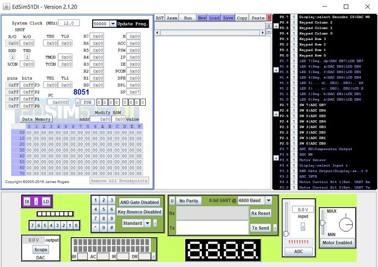
 The Virtual Peripherals:
 - Analogue-to-Digital Converter (ADC)
- Comparator
- UART
- 4 Multiplexed 7-segment Displays
- 4 X 3 Keypad
- 8 LEDs
- DC Motor
- 8 Switches
- Digital-to-Analogue Converter (DAC) - displayed on an oscilloscope
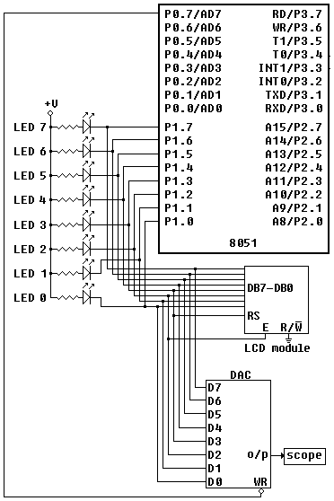
 As can be seen in the logic diagram below, the LCD Module also shares port 1 with the LEDs and DAC.
 The logic diagram shows the LED bank, DAC and LCD module connections only.
 4-bit Mode: The LCD module is a simulation of the Hitachi HD44780 and is interfaced to the 8051 in 4-bit mode. P1.7 through P1.4 are connected to DB7 through DB4, while P1.3 is connected to the register-select pin and P1.2 is connected to the enable pin. Notice the read-write pin is connected to the ground - the module can only be written to.
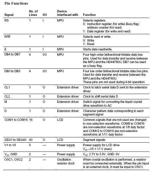
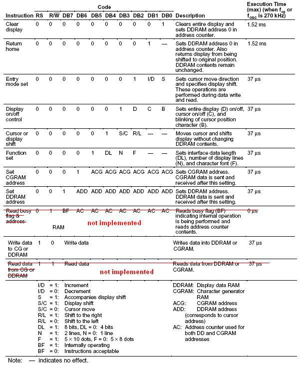
Details of the pin functions and the instructions for the LCD module are given below. For details on how to communicate with the module, see HD44780.pdf and some sample programs.
Character Blinking: Because the simulator does not run in real-time, it would be hard to know if the module was blinking. Therefore, if the programmer sets the module to blinking (see Display on/off control instruction below), the cursor position character alternates between blue text with a red background and red text with a blue background. In this way, the programmer knows at a glance if the module is in blinking mode (when not in blinking mode, all characters are black with a grey background).
The enable pin (E, connected to P1.2) is negative-edge triggered. On a negative edge on E, the module reads the data lines DB7 - DB4.
 4-bit Mode: As can be seen in the logic diagram above, the module is interfaced with the 8051 in 4-bit mode. In 4-bit mode, the module's lines DB3, DB2, DB1 and DB0 are not used. The 8-bit instruction or data must therefore be sent in two 4-bit nibbles. The high nibble is sent first, followed by the low nibble. When the enable pin is taken high and then low, this causes the module to read the pins DB7-DB4 and store them in either the IR (if an instruction is being sent - i.e., RS = 0) or the DR (if data is being sent - i.e., RS = 1).
Initially, the module is in 8-bit mode and must be set to 4-bit mode by the programmer before any other communications with the module are attempted. This is done by sending the appropriate Function Set instruction (see instruction set below).
Why send Function set twice? As stated, the module is initially in 8-bit mode, therefore the first instruction sent to it is read as an 8-bit instruction (as if DB3 - DB0 were in use). If the correct instruction is sent (with DL - on DB4 - set to zero, indicating 4-bit - see below), then the module 'knows' it is being set to 4-bit operation and it reads instructions and data in two 4-bit nibbles from then on.
4-bit Mode: As can be seen in the logic diagram above, the module is interfaced with the 8051 in 4-bit mode. In 4-bit mode, the module's lines DB3, DB2, DB1 and DB0 are not used. The 8-bit instruction or data must therefore be sent in two 4-bit nibbles. The high nibble is sent first, followed by the low nibble. When the enable pin is taken high and then low, this causes the module to read the pins DB7-DB4 and store them in either the IR (if an instruction is being sent - i.e., RS = 0) or the DR (if data is being sent - i.e., RS = 1).
Initially, the module is in 8-bit mode and must be set to 4-bit mode by the programmer before any other communications with the module are attempted. This is done by sending the appropriate Function Set instruction (see instruction set below).
Why send Function set twice? As stated, the module is initially in 8-bit mode, therefore the first instruction sent to it is read as an 8-bit instruction (as if DB3 - DB0 were in use). If the correct instruction is sent (with DL - on DB4 - set to zero, indicating 4-bit - see below), then the module 'knows' it is being set to 4-bit operation and it reads instructions and data in two 4-bit nibbles from then on.Because it reads the high nibble first, the Function set high nibble must be sent again, followed by the low nibble.
For more information, see pages 39 and 42 of HD44780.pdf. The example on page 42 is for a 1-line display, but it nonetheless explains clearly how to initialise and communicate with the module in 4-bit mode. Function Set Incorrectly: The programmer must set the module to 2-line, 5 X 8 font. The simulation of the HD44780 is implemented for 2-line, 5 X 8 font only. However, the programmer is still expected to write the code that sets the module in this mode. If the mode is not set correctly, an error message stating such is displayed, as shown here. The programmer must then reset the simulator, modify the code and try again.
 Verify that the “ABC” message appears in the LCD. (ask the demonstrator if this is not the case).
Pretty simple stuff so far, isn't it? This may seem trivially easy, but it is vital that you get a good feel for the system before you attempt anything too complicated.
Your task now is to decipher the lab1.hex code and then change it to display your own message.
Please include a Mnemonic listing of your code (with suitable comments) in your lab report.
This needn’t have many additional notes. 1 or 2 lines up at the top explaining the changes that you have made.
A brief comment on each line explaining the line-by-line changes.